Ing. Jakub Pongrácz successfully defended his doctoral thesis focused on the early stages of heteroepitaxial growth of semiconductor films.
In his research, he focused on InGaN and AlN materials, which belong to the important group of III-nitride semiconductors used in electronics and optoelectronics. One of the main problems during their preparation is the formation of crystal defects, especially threading dislocations, which can deteriorate the properties of the resulting devices.
His work compared several methods of layer preparation, specifically via chemical and physical routes, thereby showing that the conditions in the very earliest stage of growth significantly influence the final quality of the grown material. The research thus contributes to a better understanding of how semiconductor layers form and how defects that reduce the efficiency of future electronic (transistors, micro-electromechanical chips) and optoelectronic components (light-emitting diodes – LEDs, laser diodes) can be limited.
What was your doctoral thesis about?
I studied how defects form in very thin semiconductor layers on the surface of another material and what happens in the very first moments of their growth. This early stage often decides whether the resulting layer will be of high quality or whether a large number of defects will form within it.
How would you explain that to someone outside the field?
Most people today use modern, very small, and powerful chargers for phones or laptops. These are based specifically on gallium nitride (GaN). For such a component to work, we must „stack“ semiconductor atoms onto a silicon substrate with extreme precision. My work dealt with how to start this process so that instead of „crystal chaos,“ an ordered structure is formed.
Why is it important to study such defects?
Specifically, threading dislocations reduce the efficiency of the material in electronic and optoelectronic components. The dissertation shows that certain types of threading dislocations act as strong recombination centers for charge carriers, thereby directly worsening the performance of future structures.
Which materials did you study?
These were primarily InGaN and AlN semiconductor layers, so-called nitride semiconductors (compounds of nitrogen with group 13 elements of the periodic table). These materials are important for current and future semiconductor technologies because they can emit light across the entire spectral width from ultraviolet (UV-C) to infrared (IR). At the same time, thanks to their wide bandgap, they allow for very efficient energy transformation.
What was the main scientific challenge?
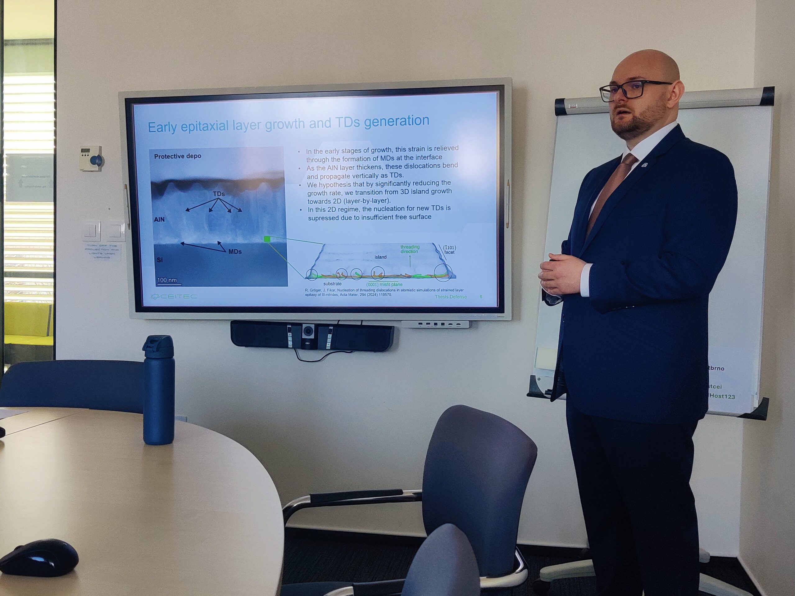
When we grow AlN or GaN on silicon, we encounter the fact that these two materials have different crystal lattice sizes – they simply do not „fit“ together (the difference is up to 19%). This creates enormous strain. If the growth is not managed correctly, this strain is released through the formation of a dense network of defects.
How did you study it?
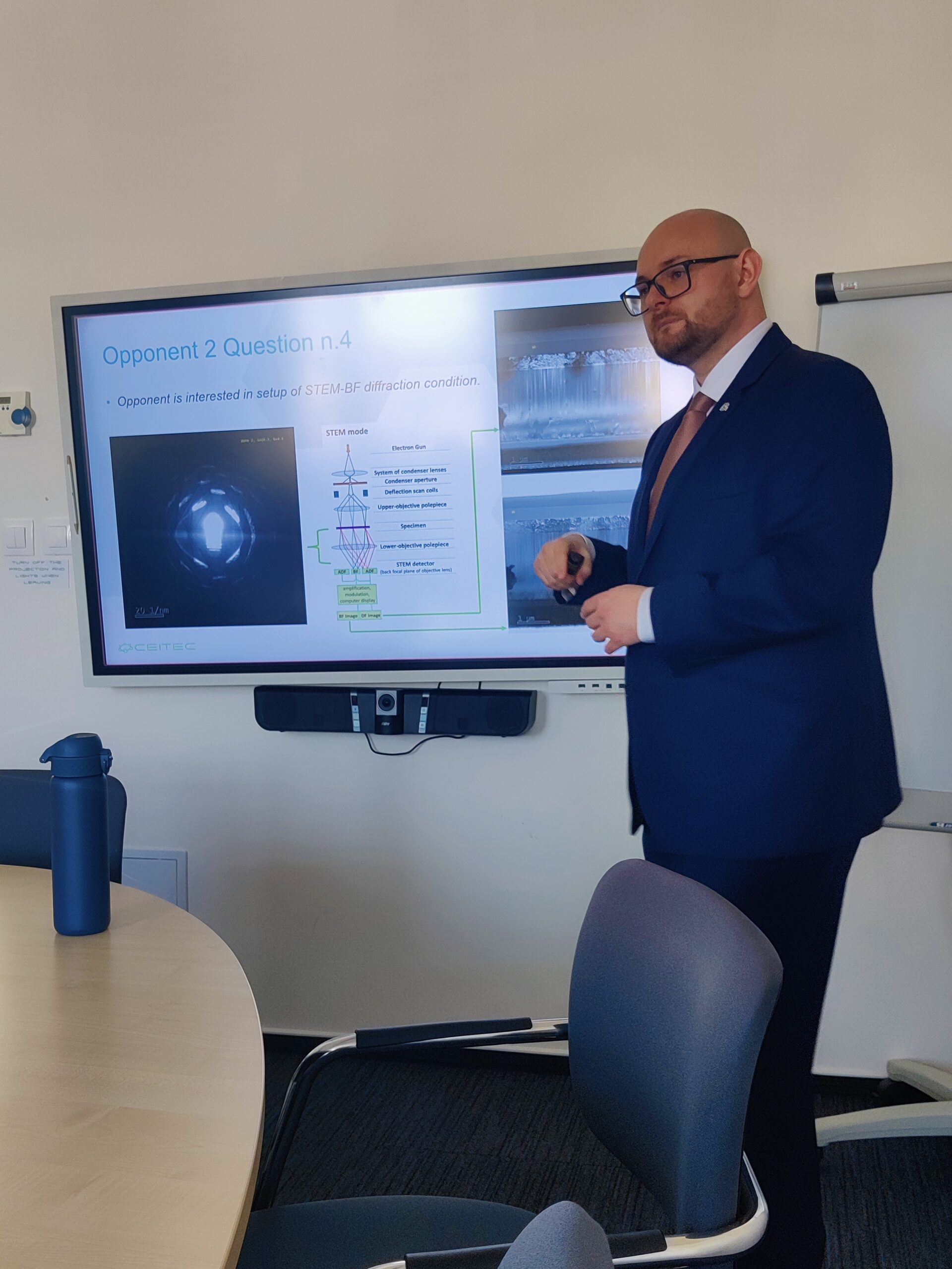
I compared several different methods of growing AlN layers using Metal-Organic Vapor Phase Epitaxy (MOVPE), Atomic Layer Deposition (ALD), and Physical Vapor Deposition (PVD). Subsequently, I observed how defects form in the material. For this, I utilized electron microscopy and other methods that allowed me to examine the surface, internal structure, and types of emerging defects.
Did the different methods lead to different results?
Yes. The work showed that individual methods lead to different morphologies and different types of defects. In layers prepared by the MOVPE method, V-pits appeared, which are the terminations of dislocations on the surface, while in PVD, island growth was more common, and in ALD, under the studied conditions, an amorphous character of the layer, higher roughness, surface inconsistency, and contamination were manifested.
Did you find a way to improve the quality?
Yes, one of the important results was that through appropriate optimization of growth conditions, it was possible to significantly reduce the density of threading dislocations in AlN layers. The dissertation describes a case where it was possible to reduce their density from values higher than 1010 cm⁻² down to 107 cm⁻².
What is the broader takeaway for the public?
My research helps develop materials for fast chargers that, thanks to high crystal quality, work more efficiently and generate almost no heat. This saves electricity and extends the lifespan of electronics. I demonstrate how precision control of atoms can create more powerful and economical technologies for everyday use.
We congratulate Jakub Pongrácz on his successful doctoral defense and wish him many more achievements in his scientific career.
The research was supported by the Czech Science Foundation (standard grant 24-12526S), the Ministry of Education, Youth and Sports of the Czech Republic through project CZ.02.2.69/0.0/0.0/18_053/0016933, the TACR TREND project “GEFSEM” No. FW01010183, the Specific Research project CEITEC VUT-J-20-6385, and the CzechNanoLab research infrastructure funded by project LM2018110.
📷 Photos: Petra Králová, CEITEC; Roman Gröger, ÚFM
 the island defects and terraces on the surface previously observed during the SEM imaging and (b) height profile along the blue line in (a) on the MOVPE-grown sample from OVGU.")
 nonporous and (b) porous sample of InGaN superlattice.")
 in which the etching occurs.")